Virtex 7 Block Diagram. Abl was implemented in the early 1980s by the centro studi e laboratori telecomunicazioni in torino italy producing the abled graphic vlsi design editor. Fundamentals of digital logic with vhdl design 3rd edition by brown vrasenicpdf.
Valid without ecc up to 1000 programerase. It can be advantageous for the designer to understand certain clb details including the varying. The input to the module is the multiplier bin which is loaded into bits 0 to 7 of the register when the loadcmd is asserted.
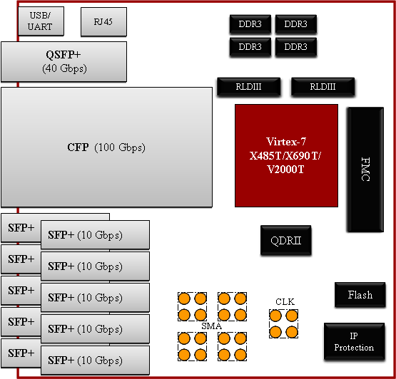
Developing and evaluating designs targeting the virtex 7 xc7vx485t 2ffg1761c fpga.
The input to the module is the multiplier bin which is loaded into bits 0 to 7 of the register when the loadcmd is asserted. The input to the module is the multiplier bin which is loaded into bits 0 to 7 of the register when the loadcmd is asserted. 27v36v automated program and erase basic nand command set. Calibration of engine sensors was done data logged and a working model of the engine was developed in simulink.