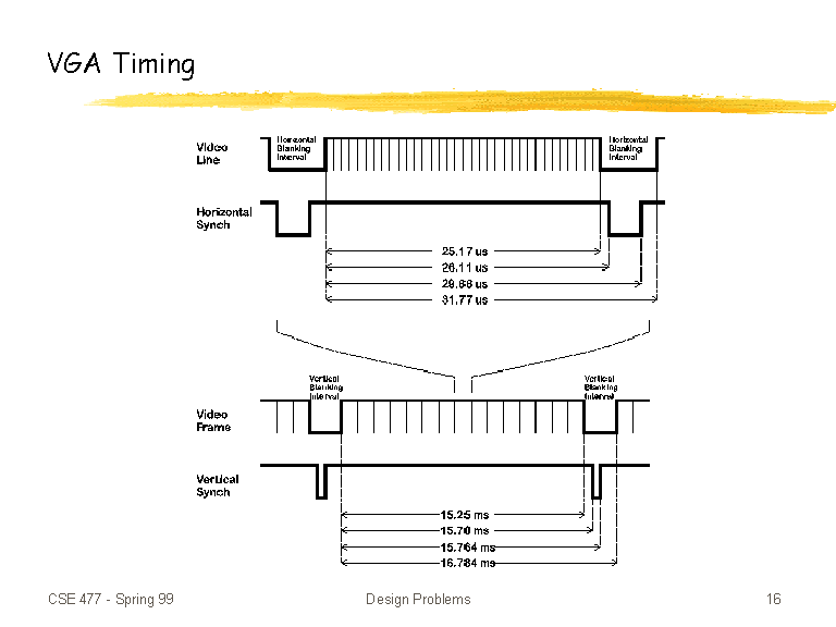
Vga Timing Diagram. The figure below shows input and output timing diagram. The ili9341 tft display board which is shown in the circuit diagram above has 14 pins the first 9 pins are for the display and the other 5 pins are for the touch module.
Setfalsepath 是用来设置 timing path表示不用 check 这些 path 的 timing但是依然会去计算这些 path 上的delay setdisabletiming 是用来设置 timing arc 表示打断这条时序弧不去计算这段时序弧的 de. External voltage regulator wiring diagram. Fully moulded beige assemblies fitted with knurled thumbscrews in monitor 9 d 15 hdd types.
Setfalsepath 是用来设置 timing path表示不用 check 这些 path 的 timing但是依然会去计算这些 path 上的delay setdisabletiming 是用来设置 timing arc 表示打断这条时序弧不去计算这段时序弧的 de.
The device can be used as a single timing and synchronization source for a system or two of them can be used as a redundant pair for improved system reliability. Power requirements active 60 mw typical 15fps. Epiphone sheraton ii wiring diagram. The device can be used as a single timing and synchronization source for a system or two of them can be used as a redundant pair for improved system reliability.