Mosfet Band Diagram. A typical diagram is shown under voltage bias in the following figure. 332 mosfet flip flop circuits131 333 random access memory devices.
332 mosfet flip flop circuits131 333 random access memory devices. Zthe corresponding band diagram is shown in figure fig4 zsilicon dioxide has a 9 ev bandgap zthis results in large band offset relative to silicon. Sze physics of semiconductor devices 1981.
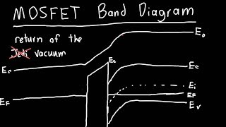
In solid state physics of semiconductors a band diagram is a diagram plotting various key electron energy levels fermi level and nearby energy band edges as a function of some spatial dimension which is often denoted x.
The slope through the oxide changes with applied v so the amount by which b is above a changes. Zthe corresponding band diagram is shown in figure fig4 zsilicon dioxide has a 9 ev bandgap zthis results in large band offset relative to silicon. Fig1 energy band diagram and mosfet internal charge distribution in accumulation region where e c conduction band energy level e f fermi energy level e v valance band energy level e i intrinsic energy level q charge of electron v g voltage applied on gate φ s surface voltage. Then we draw the vacuum level evac which is equidistant from both efs and efm since we have assumed that the metal and the semiconductor have identical work function.