Logic Diagram Of 8x1 Multiplexer. Mux is a device which is used to convert multiple. Multiplexer logical diagram.
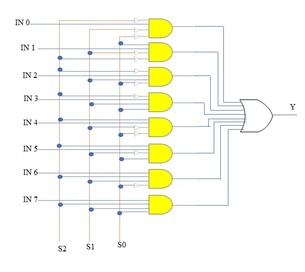
The data inputs of upper 8x1 multiplexer are i 15 to i 8 and the data inputs of lower 8x1 multiplexer are i 7 to i 0. Block diagram of a single bit 8 1 channel analog mux demux with solved draw the truth table f b c multiplexer based on equation building simple applications fpga digital circuits multiplexers ic dual 4 aims investigate circuit learn digilentinc following boolean function multiplexed imaging. The same selection lines s 2 s 1 s 0 are applied to both 8x1 multiplexers.
Try designing these using only multiplexers using similar logic to the one we saw above.
The block diagram of 8x1 multiplexer is shown in the following figure. Try designing these using only multiplexers using similar logic to the one we saw above. There are 3 variables in the given expression hence 2 n 2 3 8. Adafruit tca9548a i2c multiplexer ada2717 16 channel analog digital multiplexer.