Logic Diagram Of 4 Bit Ripple Carry Adder. When c in is fed as input to the full adder a it activates the full adder a. Instantiating 4 1 bit full adders in verilog fulladder u1 x 0 y 0 1b0 s 0 w1.
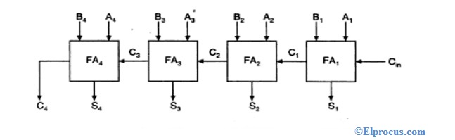
The 4 bit ripple carry adder is designed in 7. Instantiating 4 1 bit full adders in verilog fulladder u1 x 0 y 0 1b0 s 0 w1. The following figure represent the 4 bit ripple carry adder.
In the current paper the rca circuit is implemented using both 10t and 17t full adder and compared with cmos rca.
Note that the first and only the first full adder may be replaced by a half adder. Then at full adder a a 0 1 b 0 0 c in 0. In mathematics any two 4 bit binary numbers a 3 a 2 a 1 a 0 and b 3 b 2 b 1 b 0 are added as shown below using ripple carry adder this addition is carried out as shown by the following logic diagram as shown ripple carry adder works in different stages. Digital design and computer architecture begins with a modern approach by rigorously covering the fundamentals of digital logic design and then introducing hardware description languages hdls.