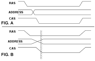
Dram Timing Diagram. To access a 64k dram device you would need sixteen address lines. The read or write of a dram is done in two main steps as illustrated in figure 7 3.
Timing diagram of a write cycle. Mode register set cycle 4. Device operations ddr2 sdram self idle setting emrs bank precharging power writing act rda read srf ref ckel emrs ckeh ckeh ckel write automatic sequence command sequence wra rda read pr pra pr refreshing refreshing down power down active with rda reading with wra active precharge.
Power on sequence and auto refresh 5.
You will then see an empty diagram. Ram timing read process choose desired word by applying address ensure rw high push chip select high and wait for a clock edge read timing cy7c102a 256k 4 static ram t aa address to valid data 12ns max t oha data hold from address change 3 ns min t acs chip select to data valid 12 ns max t cslz. Timing diagram of a write cycle. The ddr4 sdram is a high speed dynamic random access memory internally configured as sixteen banks 4 bank group with 4 banks for each bank group for x4x8 and eight banks 2 bank group with 4 banks for each bankgroup for x16 dram.