Ddr3 Timing Diagram. The block diagram of the reliable router is shown in figure 723. Aida64 cache memory benchmark understanding and prioritizing busses.
Number of views 423. This is the name used by intel to describe the socket used to hold many of their cpus. 14 revision history revision no.
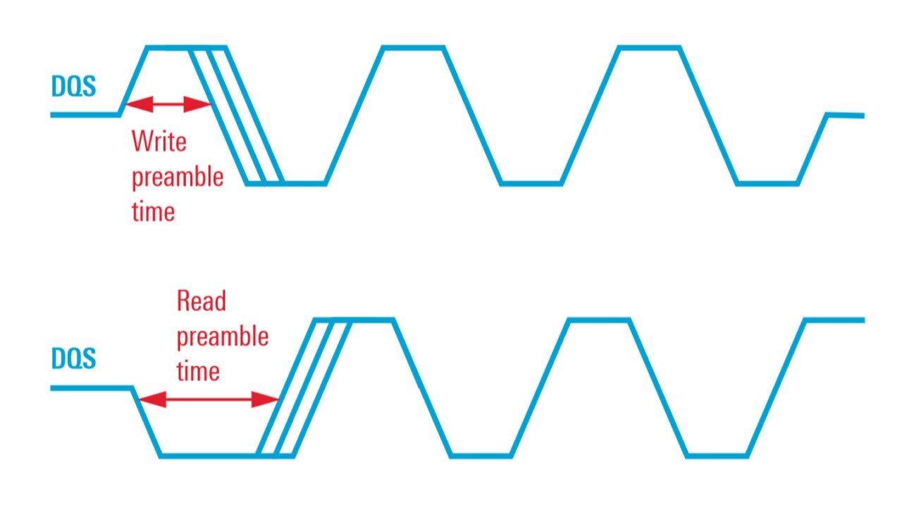
1920 subscribe send feedback ug 20115 20211206 latest document on the web.
Key timing parameters speed grade data rate mts target trcd trp cl rcd ns rp ns cl ns 1071 1866 13 13 13 1391 1391 1391 125 1600 11 11. Programmable timing parameters to support ddr3ddr3llpddr3lpddr4 sdram from various vendor advanced command reordering and scheduling to maximize bus utilization embedded dynamic drift detection in the phy to get dynamic drift compensation with the controller programmable output and odt impedance with dynamic pvt compensation. Aida64 cache memory benchmark understanding and prioritizing busses. Key timing parameters speed grade data rate mts target trcd trp cl rcd ns rp ns cl ns 1071 1866 13 13 13 1391 1391 1391 125 1600 11 11.