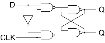
D Ff Circuit Diagram. Its state can be changed by applying the proper triggering signal. Since q a has changed from 0 to 1 it is treated as the positive clock edge by ff b.
Maintained contact conductors not connected connected disc c1 cb ls ls ls ls ls np np ls ls prs prs fs fs ps ps ts ts fls fls fts fts tgs cos pls f pls r ff r f pls 1 lo ss 12 ss 12 3 rss rss rss rss tcs off 1 2 pb pb pb pb pb pb. Our seconds count is from 0. Whats the circuit above.
Q b will be toggled at every falling edge of q a.
J and k are expressed in terms of d and qp. Answer 1 of 5. This diagram includes different electronic components with standardized representations of symbols when a symbolic circuit uses simple component images. As said earlier our clock is a 12 hour clock.