Block Diagram Qpsk. The modulation of bpsk is done using a balance modulator which multiplies the two signals applied at the input. This is called pi4 qpskthe constellation diagram of qpsk will show the constellation points lying on both x and y axesthis means that the qpsk.
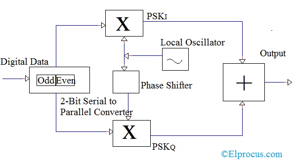
The even qpsk signal is phase shifter by 90 using a phase shifter before modulation. Turn the adder modules g control fully anti clockwise. Block diagram of cro cathode ray oscilloscope components of cro and crt with structure and working slope overload distortion and granular idle noise quantization noise in delta modulation frequency translationfrequency mixingfrequency conversionheterodyning basic concepts and need quadrature phase shift keying modulation qpsk basics waveform and.
Binary phase shift keying bpsk is a form of phase modulation using two different carrier phases to signal 1 and 0.
Bpsk system with block diagram. The set up in figure 11 can be represented by the block diagram in figure 12 below. Review the qpsk modem design on page 9. Now consider the block diagram shown in fig.