Block Diagram Of Adc0809. We believe this kind of simple block diagram adc graphic could possibly be the most trending subject later than we ration it in google help or facebook. 2all trademarks are the property of their respective owners.
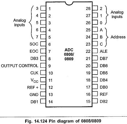
The flowchart of the ad conersion subroutine is shown in figv 3. Internal block diagram of adc0809 the various functional blocks of adc are 8 channel multiplexer comparator 256r resistor ladder switch tree successive approximation register output buffer address latch and decoder. The multiplexer uses eight standard cmos analog switches to provide for up to 8.
Lcd liquid crystal display screen is an electronic display module and find a wide range of applications.
The block diagram of the robotic end and control section is shown in figure sensors for controlling soil moisture temperature sensing the ph value for deciding. Adc0808 n adc0809 n1featuresdescriptionthe adc0808 adc0809 data acquisition component datasheet search datasheets datasheet search site for electronic. Now let us see how to interface this 8253 timer chip with the intel 8085 microprocessor. Interfaced to channel 0 of the adc0809.