Block Diagram Of 565. Is the least efficient diagram among the electrical wiring diagram. The important electrical characteristics of the 565 pll are operating frequency range.
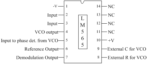
The pin diagram of ic 565 is shown in the following figure. Lm565 ic pin diagram. In the locked state the vco output frequency fo is given by f o nf s.
Out of 14 pins only 10 pins pin number 1 to 10 are utilized for the operation of pll.
Block diagram of 565 it is far more helpful as a reference guide if anyone wants to know about the homes electrical system. Pin no 2 3 signal input for phase detector. Explain the application am detector and fsk demodulator using. High linearity of modulation.