Block Diagram Bcd Adder. The rest of the connections are exactly same as those of n bit parallel adder is shown in fig. Serial binary adder is a combinational logic circuit that performs the addition of two binary numbers in serial form.
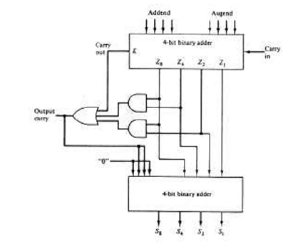
Input a 0111 b 1000 output y 1 0101explanation. K 1 z 8 0 z 4 0 z 2 0 c out 10000 c out 100 c out 1. 4 bit parallel adder.
To add 0110 to the binary sum we use a second 4 bit binary adder as shown in the figure.
Binary adder and subtraction circuits along with its various types. Two shift registers are used to store the binary numbers that are to be added. The binary adder produced the result 0001 and carried output k 1. A bcd adder is a circuit that adds two bcd digits in parallel and makes a sum digit also in bcd.