Block Diagram 74hc595. An application circuit of the ic is shown below. In that case input is feed from right side and output is getting from left side.
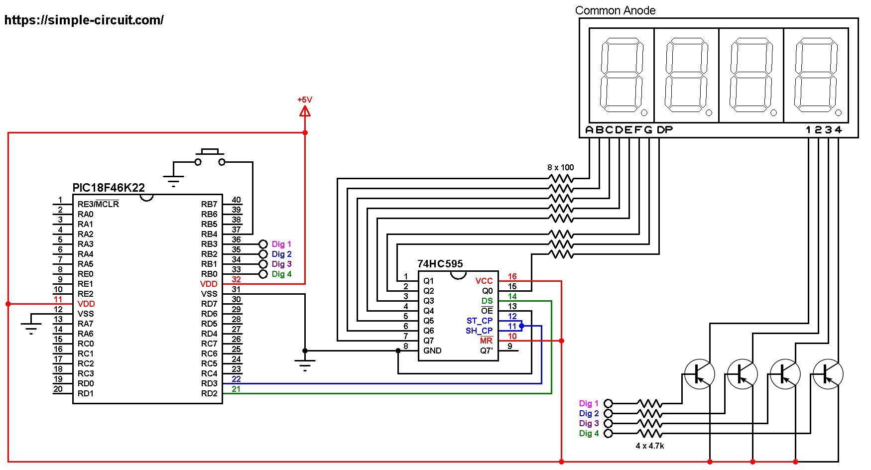
Pin number 12 ie. 74hc164 pin configuration and functions. In that case input is feed from right side and output is getting from left side.
This device possesses the high noise immunity and low power consumption of standard cmos integrated circuits as well as the ability to drive 15 ls ttl loads.
Pin number 12 ie. A block diagram of 74hc595 is shown below. 5 system block diagram. The 74hc595 shift register is commonly used with microcontrollers or microprocessors to expand the gipo functionalities.